
This is in continuation of Arduino Uno an Engineering Approach . Please go through that first to understand the background. We will validate the ATmega328P concepts with practical approach.
ATmega328/P Block Diagram
Here is the full Device or SoC(System on Chip) or Platform block diagram under discussion :

Looks complex, Lets try to divide this to several tasks and focus on one at a time.
The core microprocessor AVR
AVR got the name from its developers Alf and Vegard’s RISC processor. It is 8-bit little endian RISC processor from Atmel(Now Microchip). The program is going to execute on this Harvard Architecture RISC core.The Program Counter (PC) is 14 bits wide, thus addressing the 16 K program memory locations.

X,Y,Z are 16-bit registers used for indirect addressing. Other are 8-bit.
Device Memory MAP
Program memory :
Why should I learn this device Program memory map ? Since the device has very limited program memory. It is important to understand where this is being used and how can we optimize that for real field application.
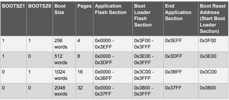
Program memory consists of bootloader and user application. Size of the program memory can be configured by FUSE setting bits BOOTSZ1 and BOOTSZ0. Please note the size in words(16-bit word). FUSE setting bytes provide a mechanism to change default reset configuration of device. We can discuss it in clock related block.
How to verify/backup existing flash program ?
Reading of flash program is not straight forward. But we can use avrdude utility after installing WinAVR . avrdude options are available here.
Note: Avoid write/program feature of avrdude directly, Otherwise you may corrupt boot loader and later require external means to re-program the same. If boot loader gets corrupted or erased , You can’t communicate with device without external debugger.

How can we verify Application code ?
I discussed the method to fetch disassembly of sketch/application data in earlier blog. The HEX data shown below is from default.hex renamed as Arduino_uno_flash_read on left side and the application program disassembly from sketch build folder.

How can I verify Boot Loader code ?
Lets compare the data in optiboot_atmega328.lst at C:\Program Files (x86)\Arduino\hardware\arduino\avr\bootloaders\optiboot\ with hex dump taken from device by avrdude.

How to verify this with Fuse bits configured ?


All fuse bytes are read as zero. That is not possible. Lets try to understand Fuse bits related to bootsz.

It seems some issue with FUSE bits reading by avrdude , so we can use a AVR library function boot_lock_fuse_bits_get()
I will discuss the code used here in next post. The output shows hfuse=0xDE .
i.e. BOOTSZ1,BOOTSZ0 = 11b
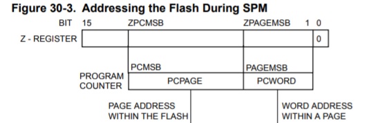
As per the boot loader table, The flash section should be from 0x3F00 to 0x3FFF. However as per build configuration it is 0x7E00-0x7FFF . Why ? As I mentioned earlier the flash bank size is given in words(16-bit) , So the address has to be shifted left by one bit i.e. 0x3F00 will become 0x7E00. This is also indicated in device datasheet section “Addressing the Flash During Self-Programming” .
References
All documents are available here. I am referring to most of these :
- Arduino Programming notebook
- Inline Assembler cookbook
- AVR Instruction set reference manual
- ATmega328P datasheet
- ATmega328P datasheet -Automotive version
- Arduino Uno board schematic
This article is discussed at Atmega328 – Arduino Uno video
Thanks for reading till end. I am trying to improve usability of my site. Did you find this discussion helpful ? If so, Please subscribe to YouTube channel Embedkari as well for additional embedded related stuff.